ASAHI KASEI
[AKD4395]
<KM063300>
1
2000/7
General Description
The AKD4395 is an evaluation board for AK4395, which is 192kHz sampling 24Bit
DAC. The AKD4395
includes a LPF which can add differential analog outputs from the AK4395 and also has a digital interface with
AKM's wave generator using ROM data and AKM's ADC evaluation boards. Therefore, it is easy to evaluate
the AK4395.
<
Ordering Guide
AKD4395 Rev.C
--- Evaluation board Rev.C for AK4395: differential output
Function
<
On-board differential output buffer circuit
<
On-board clock generator
<
BNC connector for an external clock input
<
Compatible with 3types of interface
1.
Direct interface with evaluation boards for AKM's A/D converter (AKD539X, AKD535X)
2.
Interface with a signal generator (AKD43XX)
3.
On-board CS8414 as DIR which accepts optical input.
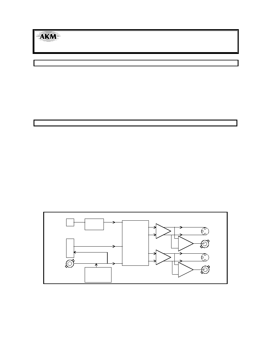
10pin Header
External
Clock
ROM Data
or
A/D input
Optical
Input
CS8414
(DIR)
Clock
Generator
AK4395
2nd Order LPF
Rch
Lch
Fig.1 Block diagram
* Circuit diagram and PCB layout are attached at the end of this manual.
(AKD4395 Rev.C is same as AKD4393 Rev.C.)
Evaluation board Rev.C for AK4395
AKD4395

ASAHI KASEI
[AKD4395]
<KM063300>
2
2000/7
<
External Analog Circuit (Rev.C)
The differential output circuit and LPF is implemented on board. The differential outputs of AK4395 is buffered by non-inverted
circuit and output via Cannon connector(differential output). LPF adds differential outputs. NJM5534D is used for op-amp on this
board that has low noise and high voltage torelance characteristics. Analog signal is output via Cannon and BNC connectors on
the board. The output level is about 2.73Vrms (typ@VREF=5.0V) by Cannon and 2Vrms (typ@VREF=5.0V) by BNC.
300
100u
300
AOUTL-
560
6.8n
330
200
6.8n
6
4
3
2
7
10u
0.1u
0.1u
10u
10u
NJM5534D
300
100u
300
AOUTL+
560
6.8
330
200
6.8n
6
4
3
2
7
10u
0.1u
0.1u
10u
NJM5534D
3
2
1
100
100
0.1u
+
NJM5534D
0.1u
10u
100
4
3
2
.2.2n
620
620
470
7
+
+
+
+
-
+
-
+
+
+
-
+
+
2.2n
Lch
-15
+15
6
470
Fig.2 External Analog Filter
<
Operation sequence
1. Set up the jumpers for power supply.
[JP15(REG)] selects power supply for AVDD pin of AK4395.
short:
5V is supplied from regulator. (default)
Nothing should be connected to A5V jack.
open:
5V is supplied from A5V.
2. Set up the power supply lines.
+15V=15V, -15V=-15V:
Power supply for op-amp. AVDD of AK4395 is supplied from "+15V" through
regulator (JP15: short).
A5V=5V:
This jack is used when AVDD of AK4395 is supplied from this. In this case, JP15
should be open.
DVDD=5V:
Power supply for logic circuit on this board.
VP=3V
5.25V:
Digital (set JP10 to VP),
AGND=DGND=0V .
Each supply line should be distributed from the power unit.
3. Set up the evaluation modes by jumper pins and DIP switches.(See next item.)
4. Power on.(The AK4395 should be reset once by bringing PD "L" upon power-up.)
*SW1 resets the AK4395 during operation.
The AK4395 is reset at SW1="L" and exits resetting at SW1="H".

ASAHI KASEI
[AKD4395]
<KM063300>
3
2000/7
<
The evaluation modes and corresponding jumper pins setting
1. Evaluation
Modes
�
Applicable Evaluation Mode
(1) DIR(Optical Link)
(2) Ideal sine wave generated by ROM data
(3) Using AD converted data
(4)All interface signals including master clock are fed externally.
(1) DIR(Optical Link) (default)
PORT2 is used for the evaluation using such as CD test disk. The DIR generates MCLK, BICK and LRCK SDATA from
the received data through optical connector(PORT2: TORX176).
Fig.3 Jumper set-up (DIR)
(2) Ideal sine wave generated by ROM data
Digital signal generated by AKD43XX are used. PORT1 is used for the interface with AKD43XX. Master clock is sent
from AKD4395 to AKD43XX then LRCK, BICK and SDATA are sent from AKD43XX to AKD4395.
JP7
S D
JP6
L R
X T L /E X T
DIR
JP5
B I
X T L /E X T
DIR
C L K
JP9
D IR
E X T
XTL
JP8
C K D IV 1
2X
1X
JP4
B C P
INV
THR
JP2
C S 8414
V D D
GND
JP1
JP14
C K D IV 2
1/2X
1X
XTL
Fig.4 Jumper set-up (ROM data)
JP7
SD
JP6
LR
XTL/EXT
DIR
JP5
BI
XTL/EXT
DIR
CLK
JP9
DIR
EXT
XTL
JP4
JP8
CKDIV1
2X
1X
BCP
INV
THR
BCP
INV
THR
(others)
(MSB
justified)
JP2
CS8414
VDD
GND
JP1
JP14
CKDIV2
1/2X
1X
XTL

ASAHI KASEI
[AKD4395]
<KM063300>
4
2000/7
(3) Using AD converted data
AD converted data from AKM's AD evaluation boards(AKD539X, AKD535X) is used through PORT1.
* In case of using external clock through a BNC connector, select EXT of JP9 and short JP1.
* In case of using the double speed sampling mode, select 1/2X of JP8 and set S2-2(DFS) on.
JP7
S D
JP6
L R
X T L /E X T
DIR
JP5
B I
X T L /E X T
DIR
C L K
JP9
D IR
E X T
XTL
JP8
C K D IV 1
2X
1X
JP4
B C P
INV
THR
JP2
C S 8414
V D D
GND
JP1
JP14
C K D IV 2
1/2X
1X
XTL
Fig.5 Jumper set-up (A/D)
(4) All interface signals including master clock are fed externally.
Under the following set-up, MCLK, LRCK and SCLK signals needed for the D/A to operate could be fed through
PORT1.
JP7
S D
JP6
L R
X T L /E X T
DIR
JP5
B I
X T L /E X T
DIR
C L K
JP9
D IR
E X T
XTL
JP8
C K D IV 1
2X
1X
JP4
B C P
INV
THR
JP2
C S 8414
V D D
GND
JP1
JP14
C K D IV 2
1/2X
1X
XTL
Fig.6 Jumper set-up (ext.)
2. MCLK
set-up
When the LRCK is fed from the 74HC4040 on the board, The ratio of MCLK to LRCK can be selected by JP8 and JP14.
JP14
JP8
X'tal
MCLK
fs
MCLK/LRCK
1X
1X
12.288MHz
12.288MHz
48kHz
256
1X
2X
24.576MHz
24.576MHz
48kHz
512
1/2X
1X
24.576MHz
12.288MHz
96kHz
128
1/2X
2X
49.152MHz
12.288MHz
96kHz
128
Table.1 set-up example
3. BICK
set-up
When BICK is supplied from U1(74HC4040), either 32fs or 64fs could be
selected. Fig.8 shows 64fs mode. 64fs mode is recommended.
*Only mode 0(LSB justified 16bit mode) can correspond to 32fs.
Fig.7 Jumper Set-up (BCS)
JP3
B C S
64
32

ASAHI KASEI
[AKD4395]
<KM063300>
5
2000/7
4. DIP switch set-up
Confirm the set-up of the DIP switch before the operation. "ON" means "H" and "OFF" means "L".
4-1.System Clock
There are two methods to set MCLK frequency. In Manual Setting Mode (ACKS = "0": Register 00H), the sampling speed is
set by DFS0/1(Table 1,4). CKS0/1/2 set the frequency of MCLK at each sampling speed (Table 2,5). In Auto Setting Mode
(ACKS = "1": Default), as MCLK frequency is detected automatically (Table 9), and the internal master clock becomes the
appropriate frequency, it is not necessary to set DFS0/1 and CKS0/1/2. In parallel mode, CKS2 and DFS1 are fixed to "0".
All external clocks (MCLK, BICK and LRCK) should always be present whenever the AK4395 is in normal operation mode (PD
= "H"). If these clocks are not provided, the AK4395 may draw excess current because the device utilizes dynamic refreshed
logic internally. If the external clocks are not present, the AK4395 should be in the power-down mode (PDN = "L") or in the
reset mode (RSTN = "0"). After exiting reset at power-up etc., the AK4395 is in power-down mode until MCLK and LRCK are
input.
Parallel Mode :
DFS0
(SW3-1)
Sampling Rate (fs)
OFF
Normal Speed Mode
30kHz~54kHz
Default
ON
Double Speed Mode
60kHz~108kHz
Table 1.Sampling Speed (Manual Setting Mode)
Note: DFS1(Register 00H) can be set at only serial mode.
Mode
ACKS
(SW4-3)
CKS1
(SW4-2)
CKS0
(SW4-1)
Normal
Double
Quad
0
OFF
OFF
OFF
256fs
128fs
N/A
Default
1
OFF
OFF
ON
256fs
256fs
N/A
2
OFF
ON
OFF
384fs
192fs
N/A
3
OFF
ON
ON
384fs
384fs
N/A
*
ON
*
*
512fs
/768fs
256fs
/384fs
128fs
/192fs
Table 2. Master Clock (Manual Setting Mode)
Note: When ACKS is ON, Auto Setting Mode is enabled.